
Main Flight Computer
Published:
Nucleus : Main Flight Computer Card
Theory of Operation
The Main Flight Computer Card (MFC) is the brain of the avionics stack. This card handles all primary functions and sends/receives data to/from all other cards in the stack.
Main Processor
A Raspberry Pi 4 Compute Module (Pi4 CM) is used as the main processor on this card. The minimum required configuration is listed below.
CM4001008 - CM4, no wireless, 1GB of RAM, 8GB of eMMC
Options for the Pi4 CM extend up to 8GB of RAM and 32GB of eMMC as well as wifi. These are easily incorporated into the HAB stack as necessary if compute requirements increase over time. This allows for changing requirements over time for the MFC as needed without major redesigns to the application processor hardware.
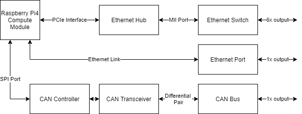
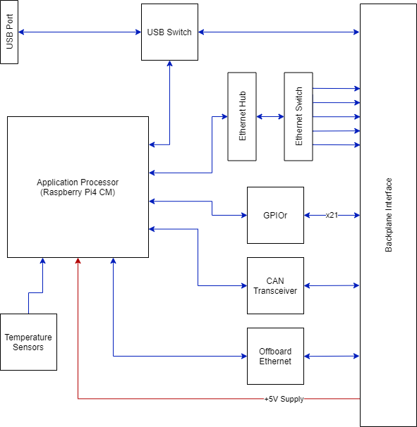
The Pi4 CM provides many of the needed interfaces for this project. Currently in use are the Ethernet, PCIe and I2C interfaces as well as the GPIO bank. The Ethernet interface is used for a direct connection to the outside world through the ground station while the PCIe link is used to interface with the Ethernet network built into the overall hardware stack. I2C is used for on card sensors and GPIO is distributed out to the rest of the cards within the stack.
The design implementation of the Pi4 CM on the MFC follows the reference design for the Pi4 CM IO board. Power and activity LEDs are present as well as Ethernet status LEDs. The Pi external reset is buffered and routed to the PCIe/Ethernet bridge. Finally a watchdog timer IC, the same as the IO board, is implemented for use as part of a Real Time Clock for the Pi.
Power for portions of the MFC is supplied by the Pi4 CM’s onboard 3.3V and 1.8V regulators. The 1.8V regulator is broken out to the MFC however it is not currently used for any circuitry. 5V is supplied from the power board through the backplane. 1.2V and 2.5V are supplied by switching regulators on the MFC itself but will be covered in the Power Management section.
While most of the signal interfaces are used for this design, options such as camera and display outputs are not broken out and there are no plans to use within the design of the MFC. Likewise, the SD card interface is also not broken out as there are no plans for using Pi4 CM’s without eMMC onboard.
Communication and Control Interfaces
PCIe Ethernet Hub Implementation From Pi4 CM to Ethernet Switch
The LAN7431 Low Power PCIe to Gigabit Ethernet Controller is implemented in this design to interface the Pi4 CM to the ETH switch. The LAN7431 was chosen as it has MII support needed for the KSZ9896CTXI switch, as one of its interfaces can only be connected over MII.
The voltage switching regulators integrated in the LAN7431 were disabled in favor of using switching regulators implemented on the MFC itself. The main benefits to this are less power dissipated in the IC itself and the supplied rails can be shared between multiple ICs. There is likely some loss in switching efficiency, however. VDDVARIO and VDD_SW_IN have the option of 3.3V and 1.8V; 3.3V was chosen to power VDDVARIO and VDD+_SW_IN as there is already a 3.3V regulator built into the Pi4 CM and can be shared with other ICs and sensors.
The LAN7431 has three configuration settings that are controlled by pull up/down resistors. These settings are read by the LAN7431 at device startup or after a reset. As these settings are controlled by resistors, a board spin would be required to properly change the configuration. Implementation of the various configuration settings follows datasheet recommendations for resistor value and using the same voltage rail as the I/O supply to the IC. The MII_EN pin is pulled high, tied to the same 3.3V rail as VDDVARIO. This configures the output of the LAN7431 for a Multimedia Independent Interface output so as to connect to the KSZ9896CTXI ethernet switch. DUPLEX and VAUX_DET are also pulled high to 3.3V, enabling full duplex communication and Power Management Event functions provided by the IC, allowing the LAN7431 to be woken from additional sleep states, respectively.
The Pi4 CM output reset is fed into the LAN7431 to provide a reset option in case the ethernet interface needs to be cycled. This is also indirectly provided to the switch through the reset output provided by the ethernet hub as well.
Finally, a 25MHz crystal was implemented for the LAN7431 per datasheet recommendations. The LAN7431’s passthrough feature is also used to provide the clock for the ETH switch, which reduced the total number of necessary clock crystals on the MFC PCB.
6 Port Ethernet Switch Implementation and Configuration
The KSZ9896CTXI 6-Port Gigabit Ethernet Switch is implemented in this design to provide connectivity to the rest of the HAB payload stack. It accepts an MII interface from the LAN7431 and provides five outputs with full gigabit PHYs, but these are only expected to be used at 10/100mbps speeds. There are also five sets of LEDs, an orange and green, providing status for the five output channels from the switch.
Power to the KSZ9896CTXI is supplied through three voltage rails, 3.3V, 2.5V, and 1.2V. VDDIO is the only rail powered by 3.3V, chosen for easy interface with the LAN7431 and anything else interfacing with the IC.
The KSZ9896CTXI is configured per the following options in the chart below:
| Pin Number | Pin Name | Configuration | Notes |
|---|---|---|---|
| 106 | LED1_1 | Pull Up (b1) | Default. Flow Control enabled |
| 90 | LED2_1 | Pull Up (b1) | Default. Normal Link up enabled |
| 82 | LED4_0 | Pull Up (b1) | Auto-negotiation disabled |
| 89 | LED2_0 | Pull Down (b0) | Auto-negotiation disabled |
| 83 | LED4_1 | Pull Down (b0) | MIIM (MDIO) Interface enabled |
| 86 | LED3_1 | Pull Down (b0) | MIIM (MDIO) Interface enabled |
| 103 | LED5_1 | Pull Up (b1) | Default. Start switch enabled |
| 77 | RXD6_3 | Pull Up (b1) | MII Interface enabled |
| 78 | RXD6_2 | Pull Up (b1) | MII Interface enabled |
| 79 | RXD6_1 | Pull Down (b0) | Default. MII Phy mode enabled |
| 80 | RXD6_0 | Pull Up (b1) | Default. 100Mbps mode enabled |
| 73 | RX_DV6/CRS_DV6/RX_CTL6 | Pull Down (b0) | Default. Disable In-Band Management |
| 75 | RX_ER6/RX_CLK6 | Pull Down (b0) | Default. 2-Wire Clock Mode |
A majority of the configuration options are set to the default options. A general description of each is provided below:
Flow control enabled: A sending station (computer or payload card) may be transmitting data faster than the other end of the link can accept it. Using flow control, the receiving station can signal the sender requesting suspension of transmissions until the receiver catches up.
Normal link up enabled: Link up time is normally determined by the time it takes to complete auto-negotiation. Additional time may be added by the auto MDI/MDI-X feature. The total link up time from power-up or cable connect is typically a second or more. Fast link up disabled (auto MDI is left enabled)
Auto-negotiation disabled: The device conforms to the auto-negotiation protocol as described by IEEE 802.3. Auto-negotiation allows each port to operate at either 10BASE-Te 100BASE-TX or 1000BASE-T by allowing link partners to select the best common mode of operation. Feature is disabled to force connection mode to simplify capacitive links
Management Interface Mode: MIIM (MDIO) was chosen to interface with the Ethernet PCIe hub.
Switch Enable at Startup: Start Switch is enabled. The switch will forward packets immediately after reset. (Default)
Port 6 Mode: MII: PHY Mode (Default)
Port 6 Speed Select: 100Mbps Mode per datasheet note (If Port 6 is configured for MII or RMII, set the speed to 100Mbps.)
In-Band Management: Disabled per default, features not required.
GMII/MII Clock Mode: 2-wire clock mode per default.
Due to design approaches taken to implement the overall hardware stack of the HAB avionics, magnetic coupling for the ethernet pairs was not implemented for the ethernet routing between PCBs through the backplane. Capacitive coupling was used instead to connect the various payload cards through ethernet to the MFC. This implementation was chosen due to the use of a backplane PCB carrying all ethernet routing, the short runs of the ethernet lines (<12” total) and the fact that all aspects of the links are controlled. This also eliminates the need for reasonably bulky magnetics, instead replaced by series capacitors and pull up resistors. APP1 through APP3 (provided below) describe the implementation of the transformer-less system used in this design.
As described in APP3 the pull up resistors on the MFC ethernet lines were chosen to maintain a level greater than 1.3V so as to generate a valid differential voltage swing that allows the ethernet transceiver to continue working properly. In the example provided, VDD is 2.5V and 40.2 ohms was selected for the resistor based on real-world resistor values close to the finalized math. Final values are 1.696V for Txdc and a swing of +/- 402mV.
Ground Station Ethernet Link (Directly From Pi4 CM)
The Ethernet output provided by the Pi4 CM is routed straight to its respective backplane connector; ETH1_TX and ETH1_RX. This is then routed to the required Ethernet jack located on the backplane for use to communicate with the outside world. The port is routed with only two ETH pairs, providing an RX and TX pair for primarily 100mbps or less connection. Routing follows the Pi4 CM datasheet recommendations of 100 ohm differential pairs and length matching of less than 50mm. These are routed off the MFC to the backplane which has a MagJack style ethernet connector.
CAN Bus Implementation
A CAN controller was required to interface between the actual CAN bus through the transceiver and the Pi4 CM. The MCP2515 was used for this purpose, chosen for its ubiquity through the maker community. The controller communicates with the Pi4 CM over SPI and is the only device on the SPI bus. A 16MHz crystal was implemented as per the datasheet to drive the internal clock/logic of the IC. The controller is powered from the 3.3V rail.
The TCAN1051 CAN transceiver is responsible for driving the differential signal pair used as the physical layer of the CAN bus network. The TCAN1051 is present on all of the cards used within the HAB payload stack. Input to the TCAN1051 is data from the MCP2515 CAN controller and output is sent off-board to the rest of the cards. The rest of the network is implemented through a simple string of devices that terminates at the power management board as it is the last possible board slot available on the backplane. The “Silent” pin on the TCAN1051 is connected to the Pi4 CM, allowing the Pi4 CM to disable transmissions to the network by disabling the transmitter if necessary, the receiver portion is still active and the MFC will continue to receive messages. The transceiver is powered through two voltage rails: 5V is used as the main power rail, driving internal circuitry and 3.3V is used to drive the communication interface so as to be able to interface with 3.3V logic on the Pi4 CM.
The final portion of the CAN circuit is the termination resistors and diode protection. Per the transceiver datasheet, a split termination was implemented with two 60.4 ohm resistors with a 4.7nF capacitor to ground tied to the common node of the two resistors. Per the datasheet, “Split termination improves the electromagnetic emissions behavior of the network by eliminating fluctuations in the bus common-mode voltages at the start and end of message transmissions.” The final portion is the diode protection, implemented through dual bi-directional TVS diodes. This diode is placed as close as possible to the connector so as to be the first point of contact in the case of a voltage transient, etc.
USB
The Rpi4 CM has a USB 2.0 interface available as an output from the module; there are two uses for this USB port on the MFC. One as a USB interface for the Rpi4 CM to connect to a PC as a USB device during development and the second use as a USB host to interface with the communications board during flight. As these two uses are expected to be exclusive of each other, i.e. will not be used at the same time, a USB switch (FSUSB42MUX) was implemented to switch the USB connection from the Rpi4 CM from the USB port on the MFC to the USB link on the backplane and vice versa. This switching is controlled through a select switch input built into the FSUSB42MUX which is tied to the output of a voltage divider supplied by the VCC pin on the MFC external USB port. When a connection is made to the external USB interface the select pin on the switch is pulled high through the voltage divider, immediately switching the connection to the external USB port. This voltage divider also pulls the Rpi4 CM USB OTG port high, signalling to the Rpi4 CM that it should be in USB device mode. When the external interface is not connected, the switch select pin is pulled low through the voltage divider, switching to the backplane USB connection and the USB OTG pin is also pulled low signalling the Rpi4 CM to be in USB host mode as the communication card’s transceiver is configured as a USB device.
GPIO Interface
Twenty-one GPIO lines are broken out from the Pi4 CM and distributed through the hardware stack. A common GPIO is shared between all cards and is expected to be used as a reset line, able to reset the entire stack. An Additional 20 GPIO are routed: three per card on the backplane and two to the balloon board for use as needed. Currently, the primary use of the GPIO is on the balloon board where the two GPIO are shorted together so the MFC can detect if there is a break in the harness to the balloon if the “receiver” GPIO no longer shows the voltage provided by the “driver” GPIO. All GPIO are pulled low through the use of 10k resistors.
Sensors
To help gather data regarding flight conditions and to provide telemetry during flight, three NTC thermistors are included on the MFC. These are located near expected “hot points” where the power dissipation will likely be highest. These thermistors are a novel design from TI and are actually silicon-based. They provide a linear resistance across temperature, eliminating the need for a linearization resistor and only requiring a pull up resistor to generate a voltage divider.
These thermistors are fed into a four-channel ADC, the TLA2024 from TI. The ADC is configured to have a full range of 4.096V as the thermistors are powered through 3.3V. In addition, the anticipated sample rate is three thermistors every 25ms; approximately 120Hz sample rate per sensor. The ADC can be configured to either 250hz or 490hz, taking Nyquist into effect to provide clean digitization of the signal, or if an additional sample rate is desired. On each input to the ADC, an RC low pass filter was implemented to reduce noise beyond the sample rate. Currently configured to 500Hz but is easily reconfigured as needed.
There is also a three-channel current monitor as part of the design. An INA3221 is used to monitor the 3.3V, 2.5V, and 1.2V rails. Inflight telemetry will be used to confirm expected power consumption and generate models for future flights. The 3.3V and 2.5V rails use 240 milliohm shunt resistors and the 1.2V rail uses a 75 milliohm resistor. Input filtering in the form of a series resistor on each sense line with a coupling capacitor between the two lines was implemented, based on the recommended design in the TI datasheet.
Power Management
While the current monitoring portion of the power design is mentioned above in the sensors section, there are two switching regulators and an e-fuse implemented in the MFC design. The TPS25942A is implemented both as protection for the card and as an additional way to reset the design through power cycling. For the fusing portion of the design, the overload trip current is set to 2A; configured by a 44.2K ohm resistor. A shutdown control method is implemented per the datasheet recommended circuit, with a series string of three resistors to generate the UVLO and OVP values and a MOSFET to control the enable line in case of need to disable the IC. Overvoltage trip point was set to 5.5V, undervoltage lockout set to 4.5V. The MOSFET is controlled by a GPIO on the Pi4 CM, and can be triggered to immediately disable power to the card. PGOOD is used as a sink for an LED and the fault line is also routed to the Pi4 CM to provide status input.
A pair of TI TLV62569 buck converters were used to supply the 2.5V and 1.2V rails required on the MFC and are supplied by the 5V rail. Designs follow the recommended implementation of the datasheet and TI’s WEBENCH Power Designer software. A secondary check of the math was performed to verify the available tools. Each regulator is expected to be at least 90% efficient and is capable of 2A output. However, the expected output is much lower, in the 100mA or less range.
Electrical Implementation
Note: Red represents power and blue represents data signals
Major components
Processor - Raspberry Pi 4 Compute Module (CM4001008)
CAN Transceiver - TCAN1051
CAN Controller - MCP2515
USB Switch - FSUSB42MUX
Ethernet Switch - KSZ9896C
Ethernet Hub - LAN7431
Voltage/current monitor - INA3221
Two/Four Channel ADC - TLA202x
E-Fuse - TPS25942A
Switching Regulator - TLV62569
Power Supplies
A list of devices per rail is provided below, as well as expected current requirements based on a power analysis of the hardware stack. The detailed analysis is available through the following google sheets link:
https://docs.google.com/spreadsheets/d/1yau7kiFFL-K1EYU-NSUKvBRh-fuvkyTJkBfG-1R5FZQ/edit?usp=sharing
12V Power Rail
- No usage
0mA current draw
5V Power Rail
- Raspberry Pi 4 Compute Module
- CAN Transceiver
- 2.5V Regulator
- 1.2V Regulator
- E-Fuse
770mA current draw
3.3V Power Rail (driven by Pi4 CM)
- Temperature Sensor
- Ethernet Switch (I/O)
- Ethernet Hub (I/O)
- CAN Transceiver
- CAN Controller
- Buffer ICs
- Ethernet LEDs
- ADCs
106mA current draw
2.5V Power Rail
- Ethernet Switch (transceivers)
- Ethernet Hub (power)
13.2mA current draw
1.2V Power Rail
- Ethernet Switch (core)
- Ethernet Hub (core)
20mA current draw
Power Considerations
Per the power analysis, it is expected that the MFC will draw approximately 4.5W of power during nominal operation. These are initial estimates and will be updated during further documentation review and board testing.
Design Implementation
The MFC is implemented as a four-layer PCB, following the stack-up provided from Macrofab as a starting point (Macrofab stackup). Copper weight is 1 oz, also following dimensions per the Macrofab stackup. Board dimensions are 100mm x 100mm, a requirement set for all payload cards as part of the HAB hardware stack. Backplane connectors are the “front” of the card and any additional IO output is on the “rear” of the card. Mounting holes are placed such that the two “rear” mounting points are 5mm from the edge in either direction, while the “front” mounting points are 5mm in from the edge on the X-axis and 15mm in from the edge on the Y-axis. The Pi4 CM is mounted through four solderable threaded posts to provide mechanical strength so as to not damage the connectors.
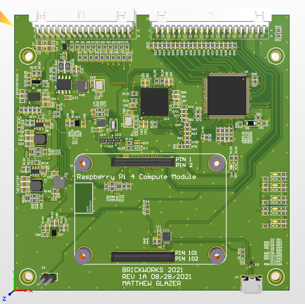
There are two differential pair implementations on the MFC: a 100 ohm and 90 ohm differential pair for the Ethernet and USB routing, respectively. These were configured through Altium using built in tools than take stackup layer values such as copper weight, base material and board thickness as input and generate the required trace width and separation values to maintain the proper differential pair impedance.
Ground pours are used throughout the PCB, these include a solid ground plane located on layer two and additional ground planes on layers one and four. Power routing is almost exclusively done through planes on layer three. Care was taken to make sure any differential routing had solid ground planes under the routing to maintain signal integrity.
Connectors
There are two 34 pin Molex MilliGrid Shrouded Right angle Connectors providing all interfaces to and from the Flight computer to the Backplane and other payload cards.
Power/GPIO Connector
Molex Part #: 0878333420
| 1 | 3 | 5 | 7 | 9 | 11 | 13 | 15 | 17 | 19 | 21 | 23 | 25 | 27 | 29 | 31 | 33 |
| 2 | 4 | 6 | 8 | 10 | 12 | 14 | 16 | 18 | 20 | 22 | 24 | 26 | 28 | 30 | 32 | 34 |
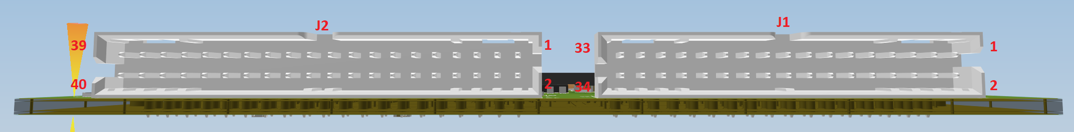
Reference view for pinout of connector is from top edge of board looking towards backplane connector.
Pin Number
Pin Function
| Pin Number | Pin Function |
|---|---|
| 1 | 12V Power Rail |
| 2 | 12V Power Rail |
| 3 | Ground |
| 4 | Ground |
| 5 | 5V Power Rail |
| 6 | 5V Power Rail |
| 7 | Ground |
| 8 | Ground |
| 9 | CAN + |
| 10 | CAN - |
| 11 | Ground |
| 12 | Ground |
| 13 | GPIO - Common |
| 14 | GPIO - 1 |
| 15 | GPIO - 2 |
| 16 | GPIO - 3 |
| 17 | GPIO - 4 |
| 18 | GPIO - 5 |
| 19 | GPIO - 6 |
| 20 | GPIO - 7 |
| 21 | GPIO - 8 |
| 22 | GPIO - 9 |
| 23 | GPIO - 10 |
| 24 | GPIO - 11 |
| 25 | GPIO - 12 |
| 26 | GPIO - 13 |
| 27 | GPIO - 14 |
| 28 | GPIO - 15 |
| 29 | GPIO - 16 |
| 30 | GPIO - 17 |
| 31 | GPIO - 18 |
| 32 | GPIO - 19 |
| 33 | GPIO - 20 |
| 34 | SPARE |
Ethernet Connector
Molex Part #: 0878334020
| 1 | 3 | 5 | 7 | 9 | 11 | 13 | 15 | 17 | 19 | 21 | 23 | 25 | 27 | 29 | 31 | 33 | 35 | 37 | 39 |
| 2 | 4 | 6 | 8 | 10 | 12 | 14 | 16 | 18 | 20 | 22 | 24 | 26 | 28 | 30 | 32 | 34 | 36 | 38 | 40 |
Reference view for pinout of connector is from FRONT of card.
Pin Number
Pin Function
| Pin Number | Pin Function |
|---|---|
| 1 | Ethernet Link 2 - RX+ |
| 2 | Ethernet Link 2 - RX- |
| 3 | Ethernet Link 2 - TX+ |
| 4 | Ethernet Link 2 - TX- |
| 5 | Ground |
| 6 | Ground |
| 7 | Ethernet Link 3 - RX+ |
| 8 | Ethernet Link 3 - RX- |
| 9 | Ethernet Link 3 - TX+ |
| 10 | Ethernet Link 3 - TX- |
| 11 | Ground |
| 12 | Ground |
| 13 | Ethernet Link 4 - RX+ |
| 14 | Ethernet Link 4 - RX- |
| 15 | Ethernet Link 4 - TX+ |
| 16 | Ethernet Link 4 - TX- |
| 17 | Ground |
| 18 | Ground |
| 19 | Ethernet Link 5 - RX+ |
| 20 | Ethernet Link 5 - RX- |
| 21 | Ethernet Link 5 - TX+ |
| 22 | Ethernet Link 5 - TX- |
| 23 | Ground |
| 24 | Ground |
| 25 | Ethernet Link 6 - RX+ |
| 26 | Ethernet Link 6 - RX- |
| 27 | Ethernet Link 6 - TX+ |
| 28 | Ethernet Link 6 - TX- |
| 29 | Ground |
| 30 | Ground |
| 31 | Ethernet Link 1 - RX+ |
| 32 | Ethernet Link 1 - RX- |
| 33 | Ethernet Link 1 - TX+ |
| 34 | Ethernet Link 1 - TX- |
| 35 | Ground |
| 36 | Ground |
| 37 | USB 2.0 - D- |
| 38 | USB 2.0 - D+ |
| 39 | SPARE |
| 40 | SPARE |
References
Whitepapers and App Notes
APP1: AN-1519 DP83848 PHYTER Transformerless Ethernet Operation
APP2: Transformerless Applications of Microchip’s Ethernet Devices
APP3: Capacitive Coupling Ethernet Transceivers without Using Transformers
APP4: LAN7431 Hardware Design Checklist