
Avionics Sensor Card
Published:
Nucleus : Avionics Sensor Card
Theory of Operation
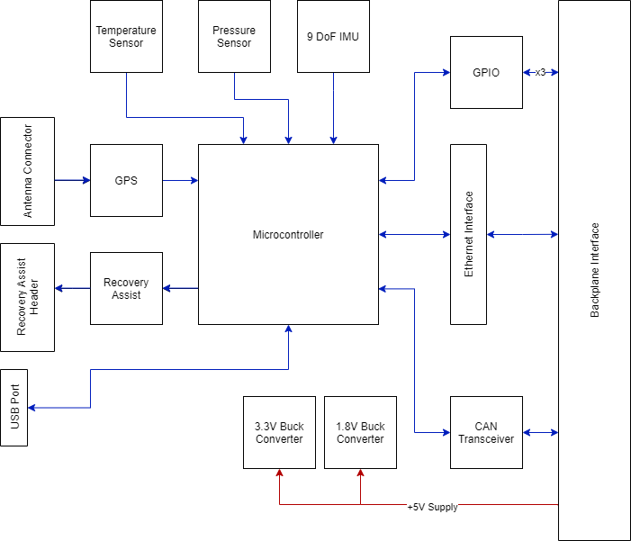
This card is the “eyes and ears” of the Main Flight Computer Card and contains all interfaces that are beyond the main processing and network management of the MFC. All sensors, interfaces and control systems used by the MFC directly and not in coordination with a payload mission exist on this card.
Main Processor
The Balloon Board, and other payload cards, has an STM32 microcontroller as its main processor. The STM32F407VET6TR is a single core, 168 MHz 32 bit Cortex M4 processor. A variety of features were desired from a microcontroller for the various payload cards, including Ethernet, USB, CAN, Timers and GPIO. The biggest driver for part selection was primarily the Ethernet and CAN requirements, as well as sharing the same microcontroller across all payload cards.
The balloon board uses the following options from the STM32F407VET6TR
- 10x GPIO pins
- 1x ADC inputs
- USB Controller
- CAN Controller
- I2C Interface
- UART Interface
- JTAG Interface
All options are configured through STMicro’s CubeMX software and validated through said software to confirm no conflicts between I/Os and various modules. A Power estimate was also generated as an initial estimate for the power consumption of the microcontroller.
The 10 GPIO lines operate a handful of features including sensor interrupts and data ready flags, power management alerts and disable commands and finally GPIO from the MFC. ADC inputs accept E-Fuse analog current telemetry for conversion to their respective digital values. USB was implemented to assist programming and debugging. JTAG was implemented for initial programming and loading a bootloader. CAN is implemented for off card communication, as described in the CAN Bus Implementation section. I2C is implemented to communicate with sensors located on the Balloon Board. UART is used for the GPS receiver interface.
The design implementation of the microcontroller follows a hardware implementation guide provided by STMicro. The microcontroller has two oscillators: a high speed 25 MHz crystal used for the core clock and a low speed 32.768 kHz crystal used for a Real Time Clock. The 25 MHz clock generated is fed into a PLL within the microcontroller that drives the 168 MHz core clock and various other clocks used for other components within the microcontroller. There is one external resistor configurable setting on the microcontroller, the boot mode selection. As the intent is to use the main flash memory as a boot space the BOOT0 pin, pin 94, is tied to ground using a 10k pull down resistor. This also avoids any issues with user code interacting with the bootloader as the boot loader is stored in system memory, which is an available option for a boot location. The external reset, nRST, for the microcontroller is broken out to a button on the PCB and a two pin header for other uses. As this is an active low signal, the signal is pulled high through a 10k pull up resistor.
Finally the microcontroller is supplied by 3.3V for all voltage rails within the microcontroller, this includes the VDD, VBAT and VDDA/VREF rails. VBAT is used as a backup supply for the microcontroller but as there is no plans to use that feature it is tied to the same voltage rail that supplies VDD. All supplies follow guidelines for decoupling capacitors, including VDD which requires a larger 4.7uF bulk capacitor at the connection point to the 3.3V supply rail, which then supplies each of the VDD pins on the IC, i.e. each of the IC’s power pins connect not directly to the 3.3V supply but through a trace that goes to the 4.7uF capacitor first.
Communication and Control Interfaces
Ethernet PHY
The KSZ8081MNX Ethernet Physical Layer Transceiver is implemented in this design to interface the microcontroller with the rest of the Ethernet networking present within the HAB avionics stack. It accepts an MII interface from the microcontroller and provides a single ethernet output through its PHY. The KSZ8081MNX is capable of 10/100mbps with an RX and TX output pair. Two green LEDs provide status for the IC output/network activity.
Power to the KSZ8081MNX is supplied through one voltage rail, 3.3V. While 3.3V is supplied to the PHY, it internally generates a 1.2V supply to power the core of the KSZ8081MNX. The 1.2V rail is decoupled externally but used exclusively for internal circuitry.
The KSZ8081MNX is configured per the following options in the chart below. Following datasheet recommendations a 1k resistor is used as a pull down resistor where needed. Datasheet recommends a 4.7k resistor for a pull up but a 10k was selected instead.
| Pin Number | Pin Name | Configuration | Notes |
|---|---|---|---|
| 15 | PHYAD2 | Pull Down (b0) | Default. PHY Address set to 1 |
| 14 | PHYAD1 | Pull Down (b0) | Default. PHY Address set to 1 |
| 13 | PHYAD0 | Pull Up (b1) | Default. PHY Address set to 1 |
| 19 | CONFIG2 | Pull Down (b0) | Config Mode set to MII interface |
| 29 | CONFIG1 | Pull Down (b0) | Config Mode set to MII interface |
| 28 | CONFIG0 | Pull Down (b0) | Config Mode set to MII interface |
| 20 | ISO | Pull Down (b0) | Default. Disable isolate mode |
| 31 | SPEED | Pull Up (b1) | Default. Enable 100Mbps |
| 16 | DUPLEX | Pull Down (b0) | Enable Full-Duplex |
| 30 | NWAYEN | Pull Down (b0) | Disable auto-negotiation |
| 19 | B-CAST_OFF | Pull Down (b0) | Default. PHY Address 0 set as broadcast PHY address |
| 21 | NAND_Tree# | Pull Up (b1) | Default. NAND Tree disabled |
A majority of the configuration options are set to the default options. A general description of each is provided below:
- PHYAD: Default PHY address configured to be “1”. Options range up from 0 to 7. 0 is reserved as the broadcast address and avoided.
- CONFIG: Default Communications mode. Interface is set to MII. Other option is for the device to communicate directly to another KSZ8081MNX, which is not how this system is implemented
- ISOLATE: Default isolation mode. Isolation mode disables the connection between the MII interface and the transmit interface. Commonly used for debugging and can be configured in software if ever needed.
- SPEED: Default speed mode. Speed is configured for 100Mbps.
- DUPLEX: Full-Duplex mode enabled. Allowing bidirectional communication, enabling the transmitter and receiver to be active simultaneously.
- NWAYEN: Auto-negotiation disabled. Device follows ethernet protocol implementation allowing for adaptive speed settings, i.e. the ethernet link generated by the IC and its downstream connection can negotiate a speed. Disabled due to capacitive link requirement
- B-CAST_OFF: Default state. PHY address 0 configured to be broadcast PHY address.
- NAND_Tree#: Default tree configuration. Used for fault detection between IC I/O and board. default state of disabled and if needed can be configured in software.
The PHY reset is controllable from the microcontroller, providing a way to cycle the PHY if necessary, in addition the PHY provides an interrupt output back to the microcontroller.
A 25MHz crystal was implemented for the KSZ8081MNX to generate an internal reference clock. Implementation follows datasheet recommendations.
CAN Bus Implementation
The TCAN1051 CAN transceiver is responsible for driving the differential signal pair used as the physical layer of the CAN bus network. The TCAN1051 is present on all of the cards used within the HAB payload stack. Input to the TCAN1051 is data from the STM32 microcontroller and output is sent off-board to the rest of the cards. The rest of the network is implemented through a simple string of devices that terminates at the power management board as it is the last possible board slot available on the backplane. The “Silent” pin on the TCAN1051 is connected to the microcontroller, allowing the microcontroller to disable transmissions to the network by disabling the transmitter if necessary. The receiver portion is still active and the Balloon Board will continue to receive messages even if the silent pin is active. The transceiver is powered through two voltage rails: 5V is used as the main power rail, driving internal circuitry and 3.3V is used to drive the communication interface so as to be able to interface with 3.3V logic on the STM32 microcontroller.
The microcontroller has two CAN interfaces, of which only one is only used in this design. These support up to 1 Mbit/s and fully support the CAN 2.0A and B specifications.
USB
The STM32 Microcontroller has a USB 2.0 interface available as one of its communication outputs. The expected use case for the USB output is to directly interface with a computer for programming tasks as well as telemetry during development. The USB input as implemented on the PCB does not provide power to the system, only powering an LED to show good connection. USB functionality available after adding a bootloader to the microcontroller, i.e. after initial programming of the device after assembly.
GPIO Interface
The Avionics Sensor Card receives three GPIO lines from the MFC through the backplane, two discrete GPIO and the common GPIO pin used as a reset system for the HAB electronics. The two discrete GPIO are routed to the microcontroller. The common GPIO is used as a system reset.
Sensors
The three main sensors, IMU, pressure and temperature are the main inputs of flight data to the MFC. These sensors will be used in relation to all activities the HAB performs. Other similar sensors may be implemented but only if specifically required. I.e. the Balloon Board provides a secondary set for additional data and the Altitude Control/Dynamics card also has a set.
An ICM-20948 9 axis IMU was implemented to capture movement of the payload during flight. The sensor is made up of a three axis accelerometer, gyroscope and magnetometer. This will allow for both positional/movement information of the payload and allow for comparison against the similar data captured from the balloon. The ICM-20948 is supplied from the 1.8V rail and communicates with the MCU through I2C. A GPIO acting as an interrupt is connected to the MCU for data ready and similar commands. The IMU’s I2C address is 0x68h.
A BMP388 is also part of sensor suite on the Sensor Card, this sensor will capture pressure values during flight and acts as an altimeter. Similar to the IMU this gives a second data point along with the balloon, allowing for better models of the HAB flight. the BMP388 is supplied from the 1.8V rail and communicates with the MCU through I2C. A GPIO acting as an interrupt is connected to the MCU for data ready and similar commands. The pressure sensor’s I2C address is 0x76h.
A TMP117 temperature sensor makes up the final sensor of the general set of sensors; the IMU, pressure sensor and this temperature sensor. This is a high accuracy digital temperature sensor, capable of +/- 0.1C measurements over a range of -20C to 50C. The TMP117 is supplied from the 3.3V rail and communicates with the MCU through I2C. An alert pin from the sensor to the microcontroller provides an interrupt for over temperature warnings or data ready signals. The temperature sensor’s I2C address is 0x48h.
As there are multiple sensors on powered through either the 1.8V or 3.3V rail and their respective I/O outputs from the same voltage rails, it was required to implement a level shifter for the I2C network on the Avionics Sensor Card. This was accomplished through the use of the PCA9306, a bi-directional level shifter designed for I2C networks. This allows for the 1.8V supplied sensors to communicate with the microcontroller without damaging their communication interfaces or causing errors due to not hitting the correct input high and low voltages to the microcontroller’s I2C interface.
To help gather data regarding flight conditions and to provide telemetry during flight, three NTC thermistors are included on the Avionics Sensor Card. These are located near expected “hot points” where the power dissipation will likely be highest. These thermistors are a novel design from TI and are actually silicon-based. They provide a linear resistance across temperature, eliminating the need for a linearization resistor and only requiring a pull up resistor to generate a voltage divider.
These thermistors are fed into a four-channel ADC, the TLA2024 from TI. The ADC is configured to have a full range of 4.096V as the thermistors are powered through 3.3V. In addition, the anticipated sample rate is three thermistors every 25ms; approximately 120Hz sample rate per sensor. The ADC can be configured to either 250hz or 490hz, taking Nyquist into effect to provide clean digitization of the signal, or if an additional sample rate is desired. On each input to the ADC, an RC low pass filter was implemented to reduce noise beyond the sample rate. Currently configured to 500Hz but is easily reconfigured as needed.
There are also two single-channel current monitors as part of the design. the INA219 is used to monitor the 3.3V, and 1.8V rails. Inflight telemetry will be used to confirm expected power consumption and generate models for future flights. The 3.3V and 1.8V rails use 240 milliohm shunt resistors. Input filtering in the form of a series resistor on each sense line with a coupling capacitor between the two lines was implemented, based on the recommended design in the TI datasheet.
External Interfaces
This card provides one distinct external interfaces, one for GPS and one for Recovery Assistance
GPS
Provides an SMA header for the antenna connected to the GPS antenna. This GPS unit provides the HAB with its own GPS tracking and will eventually become the primary input for GPS. Currently this subsystem will act as the secondary, backup to the APRS tracking provides by a COTS board.
Power Management
While the current monitoring portion of the power design is mentioned above in the sensors section, there are three switching regulators and and two E-Fuses implemented on the Balloon Board design. The TPS25942A is implemented both as protection for the card and as an additional way to reset the design through power cycling. For the fusing portion of the design, on the 5V rail, the overload trip current is set to 600mA; configured by a 150K ohm resistor. A shutdown control method is implemented per the datasheet recommended circuit, with a series string of three resistors to generate the UVLO and OVP values and a MOSFET to control the enable line in case of need to disable the IC. Overvoltage trip point was set to 5.5V, undervoltage lockout set to 4.5V for the 5V rail. For the E-Fuses, the NMOS FET is controlled by a GPIO on the microcontroller, and can be triggered to immediately disable power to the card. For the 5V E-Fuse, the MFC can also command the FET as part of the system reset through the common GPIO. The two inputs are part of a diode OR to avoid any crosstalk or backfeed from the two signals. PGOOD is used as a sink for an LED for status on both E-Fuses.
A pair of TI TPS6215x buck converters were used to supply the 3.3V and 1.8V rails required on the Balloon Board and are supplied by the 5V rail. Designs follow the recommended implementation of the datasheet and TI’s WEBENCH Power Designer software. A secondary check of the math was performed to verify the available tools. The TPS62151 is designed for a fixed output of 3.3V and TPS62152 for an output of 1.8V. Each regulator is expected to be at least 90% efficient. The TPS6215x are capable of 1A output. However, the expected output for the 3.3V and 1.8V rails is significantly lower, in the 100mA or less range.
Electrical Implementation
Note: Red represents power and blue represents data signals
Major components
Microcontroller - STM32F407VET6TR
CAN Transceiver - TCAN1051
Pressure Sensor - BMP388
9 DoF IMU - ICM-20948
Temperature Sensor - TMP117A
Thermistors - TMP61
Two/Four Channel ADC - TLA202x
GPS Receiver - MAX-M8Q-0-10
Ethernet PHY - KSZ8081MNX
Voltage/current monitor - INA219
E-Fuse - TPS25942A
5V Switching Regulators - TPS62151
Power Supplies
A list of devices per rail is provided below, as well as expected current requirements based on a power analysis of the hardware stack. The detailed analysis is available through the following google sheets link:
Hardware Stack Power Analyses
12V Power Rail
- No expected usage
0mA current draw
5V Power Rail
- 3.3 Switching Regulator
- 1.8V Switching Regulator
- CAN Transceiver
- E-Fuse
89mA current draw
3.3V Power Rail
- Ethernet Transceiver
- CAN Transceiver
- GPS Receiver
- Microcontroller
- Temperature Sensor
- ADC
- Current Sensor
115mA current draw
1.8V Power Rail
- IMU
- Pressure Sensor
4.5mA current draw
Power Considerations
Per the power analysis, it is expected that the Avionics Sensor Card will draw approximately 558 mW of power during nominal operation. These are initial estimates and will be updated during further documentation review and board testing.
Design Implementation
Connectors
There is one 28 pin Molex MilliGrid shrouded right angle connector providing all interfaces to and from the Avionics Sensor Card to the Backplane and Main Flight Computer.
Backplane
Molex Part #: 0878332820
| 1 | 3 | 5 | 7 | 9 | 11 | 13 | 15 | 17 | 19 | 21 | 23 | 25 | 27 | 29 | 31 | 33 |
| 2 | 4 | 6 | 8 | 10 | 12 | 14 | 16 | 18 | 20 | 22 | 24 | 26 | 28 | 30 | 32 | 34 |
Reference view for pinout of connector is from top edge of board looking towards backplane connector.
Pin Number
Pin Function
| Pin Number | Pin Function |
|---|---|
| 1 | 12V Power Rail |
| 2 | 12V Power Rail |
| 3 | Ground |
| 4 | Ground |
| 5 | 5V Power Rail |
| 6 | 5V Power Rail |
| 7 | Ground |
| 8 | Ground |
| 9 | CAN + |
| 10 | CAN - |
| 11 | Ground |
| 12 | Ground |
| 13 | GPIO - Common |
| 14 | GPIO - 1 |
| 15 | GPIO - 2 |
| 16 | GPIO - 3 |
| 17 | SPARE |
| 18 | SPARE |
| 19 | SPARE |
| 20 | SPARE |
| 21 | SPARE |
| 22 | SPARE |
| 23 | Ground |
| 24 | Ground |
| 25 | Ethernet Link 1 - TX+ |
| 26 | Ethernet Link 1 - TX- |
| 27 | Ethernet Link 1 - RX+ |
| 28 | Ethernet Link 1 - RX- |